
 The proverbial saying “garbage in, garbage out” holds true in the electronic product development world. PCB designers stand squarely in the middle of a busy information intersection flowing with inputs and outputs. Missing or bad information at the beginning of a design project will undoubtedly lead to board respins, increased costs, and most importantly, a delayed product release. The same can be said about the PCB designer who doesn’t provide a fully checked and comprehensive data package to the downstream manufacturers, i.e., “throwing it over the fence.”
The proverbial saying “garbage in, garbage out” holds true in the electronic product development world. PCB designers stand squarely in the middle of a busy information intersection flowing with inputs and outputs. Missing or bad information at the beginning of a design project will undoubtedly lead to board respins, increased costs, and most importantly, a delayed product release. The same can be said about the PCB designer who doesn’t provide a fully checked and comprehensive data package to the downstream manufacturers, i.e., “throwing it over the fence.”
 Once a design project begins, the PCB designer will inevitably have questions or concerns about something in the input package – an obvious schematic error, mechanical conflict, etc. Although a phone call is great, we have found sometimes engineers would rather communicate via email. We find it better to keep emails short and concise. Lengthy emails with too many questions (more than three) will generally result in some questions going unanswered.
On extra-large design projects that may span many months, there can be literally hundreds of emails, most with very important information from a variety of stakeholders. In these cases, it is very easy due to a variety of reasons, for an instruction to be missed or forgotten. We find it best to organize these emails by moving them into a Word or Excel document where they can be tracked through a typical color-coding system (red, yellow, and green) to ensure nothing gets missed.
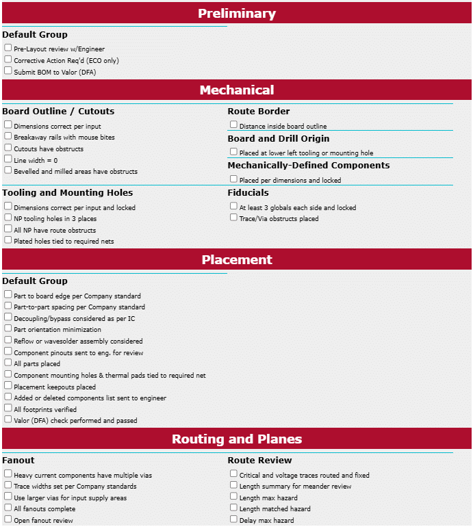
Finally, as part of our quality process, we rely on a series of checks and balances to ensure we haven’t missed any critical information from getting into the design database, as well as to ensure we are not “throwing incomplete data over the fence” to one of our downstream manufacturing friends. First, we insist with our designers that all the mechanical, electrical, and manufacturing constraints/rules are embedded into the design database. I’m always amazed when we receive a customer’s database that requires edits, or the previous designer did not enter the routing constraints into the tool. Without doing this, it is virtually impossible to say for certain that all the rules have been met. Also, as an iterative process and discipline throughout the design project, our designers have a formal checklist of 90+ items that must be reviewed and/or considered at the different phases of the project, such as the following items:
Once a design project begins, the PCB designer will inevitably have questions or concerns about something in the input package – an obvious schematic error, mechanical conflict, etc. Although a phone call is great, we have found sometimes engineers would rather communicate via email. We find it better to keep emails short and concise. Lengthy emails with too many questions (more than three) will generally result in some questions going unanswered.
On extra-large design projects that may span many months, there can be literally hundreds of emails, most with very important information from a variety of stakeholders. In these cases, it is very easy due to a variety of reasons, for an instruction to be missed or forgotten. We find it best to organize these emails by moving them into a Word or Excel document where they can be tracked through a typical color-coding system (red, yellow, and green) to ensure nothing gets missed.
Finally, as part of our quality process, we rely on a series of checks and balances to ensure we haven’t missed any critical information from getting into the design database, as well as to ensure we are not “throwing incomplete data over the fence” to one of our downstream manufacturing friends. First, we insist with our designers that all the mechanical, electrical, and manufacturing constraints/rules are embedded into the design database. I’m always amazed when we receive a customer’s database that requires edits, or the previous designer did not enter the routing constraints into the tool. Without doing this, it is virtually impossible to say for certain that all the rules have been met. Also, as an iterative process and discipline throughout the design project, our designers have a formal checklist of 90+ items that must be reviewed and/or considered at the different phases of the project, such as the following items:
 In conclusion, likely the most important way to help eliminate “garbage in, garbage out” is to have a detailed-oriented, experienced designer at the helm that understands today’s electrical and manufacturing technologies. It’s not bad or missing data if the PCB designer receiving the information doesn’t recognize it as such. Although, some things may be beyond PCB designers’ control.
But by standing in that busy information intersection, experienced designers who utilize documented standards, effective and proactive communication, and a system of checks and balances can do their part to reduce or even eliminate bad or missing data.
In conclusion, likely the most important way to help eliminate “garbage in, garbage out” is to have a detailed-oriented, experienced designer at the helm that understands today’s electrical and manufacturing technologies. It’s not bad or missing data if the PCB designer receiving the information doesn’t recognize it as such. Although, some things may be beyond PCB designers’ control.
But by standing in that busy information intersection, experienced designers who utilize documented standards, effective and proactive communication, and a system of checks and balances can do their part to reduce or even eliminate bad or missing data.

