
Should we be passionate about this? YES…Why?
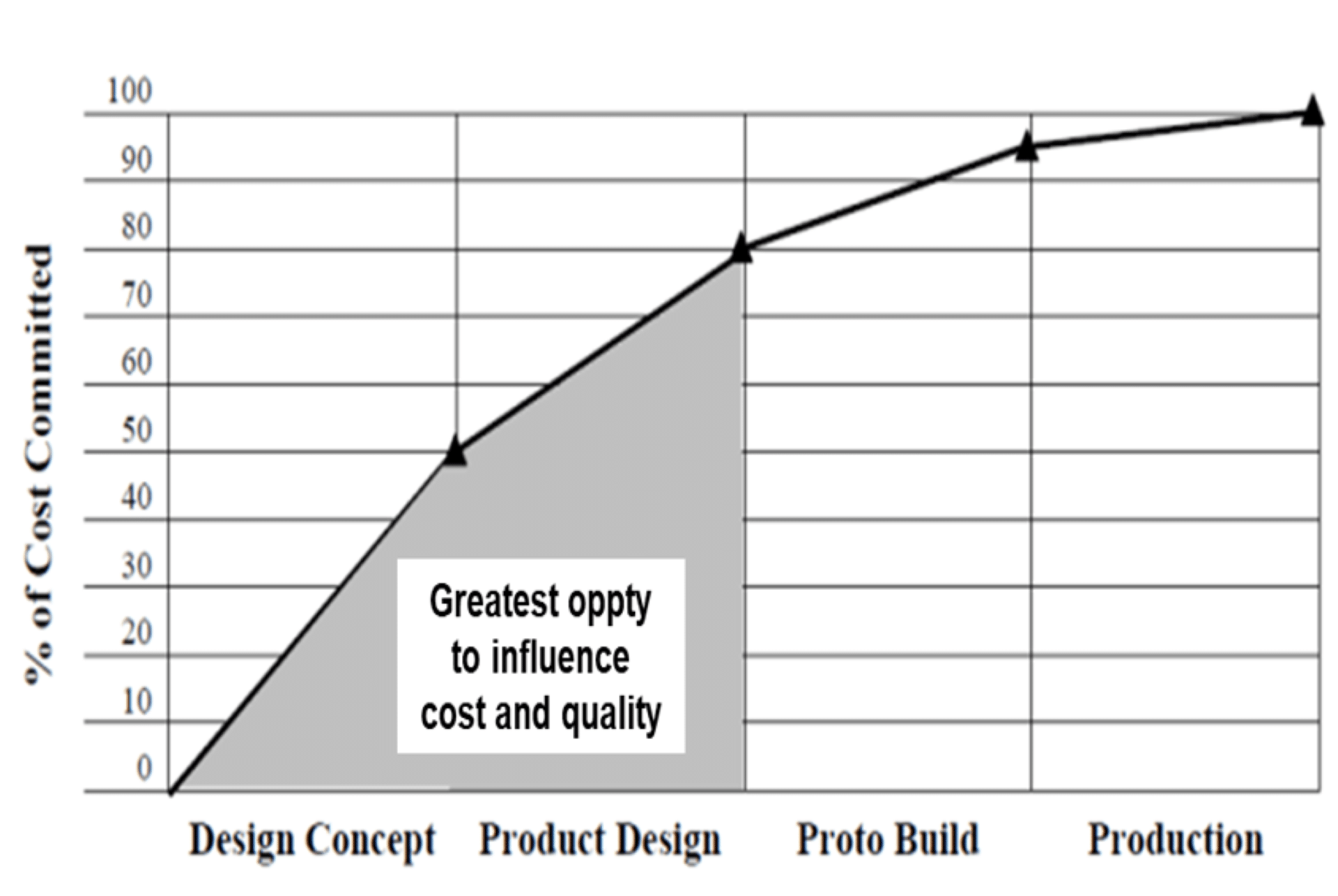
Because 75–80% of a new product’s cost and “designed‑in quality” is determined and semi-anchored before the prototype build even begins.
That means your greatest opportunity to influence reliability, manufacturability, cost, and speed-to-market happens early, very early, which is critical to consistently achieving OTD and quality goals.
DFM is not an optional step. It’s the foundation for product stability, repeatability, and long-term lifecycle success.
Our Role in DFM
We help turn design intent into manufacturing success. Our DFM activities deliver rigorous manufacturability assessments and production-readiness insight that reduce risk and enable confident execution. Although PCB design ownership remains with the customer and some sites do not provide design services, every site actively collaborates with Emerald’s internal design service teams and maintains strong, trusted relationships with leading external design partners.
By combining proven preview methodologies with deep engineering expertise, we deliver clear, high-value recommendations for customer evaluation and implementation.
DFMs Are Based On:
Industry Standards- IPC‑2221 – Generic standard for PCB design
- IPC‑7095 – Design and assembly for BGAs
- IPC‑7525 – Stencil design guidelines
- IPC‑SM‑7531 – Surface-mount design practices
- Valor DFM analysis
- Team of product and process engineers with decades of manufacturing experience
DFM Process on PCBA: Our 3-Step Process
STEP 1: Fab Review (Pre-Route)
Focus – Major component placement
- Identify high-impact issues early
- Review component clearances, orientations, and process-critical features
- Discuss initial findings with the customer
STEP 2: Fab Review (Post-Route)
Focus – Full component placement
- Deep-dive analysis on final placement and routing
- Evaluate manufacturing risk areas using Valor and internal expertise
- Review concerns and recommendations with the customer
Addressing potential issues before the board is released to fabrication saves time and costs and prevents avoidable quality problems.
STEP 3: Product Build & Ongoing DFM
Once the board enters production:
- Extensive process and product quality data is collected
- Internal cross-functional teams assess DFM vs. non-DFM issues
- Findings are shared with customers in ongoing reviews to continuously improve future builds
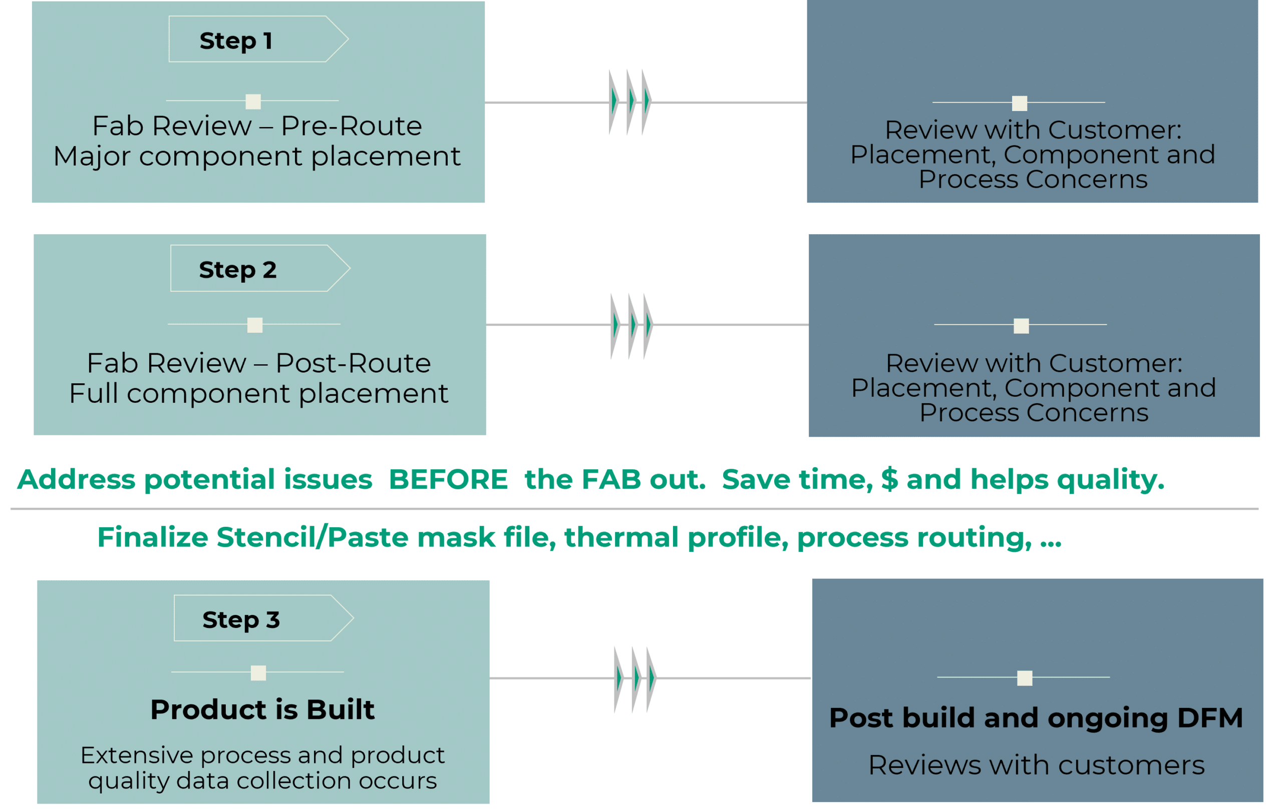
Reporting granularity and analytics availability may vary by site and project scope.
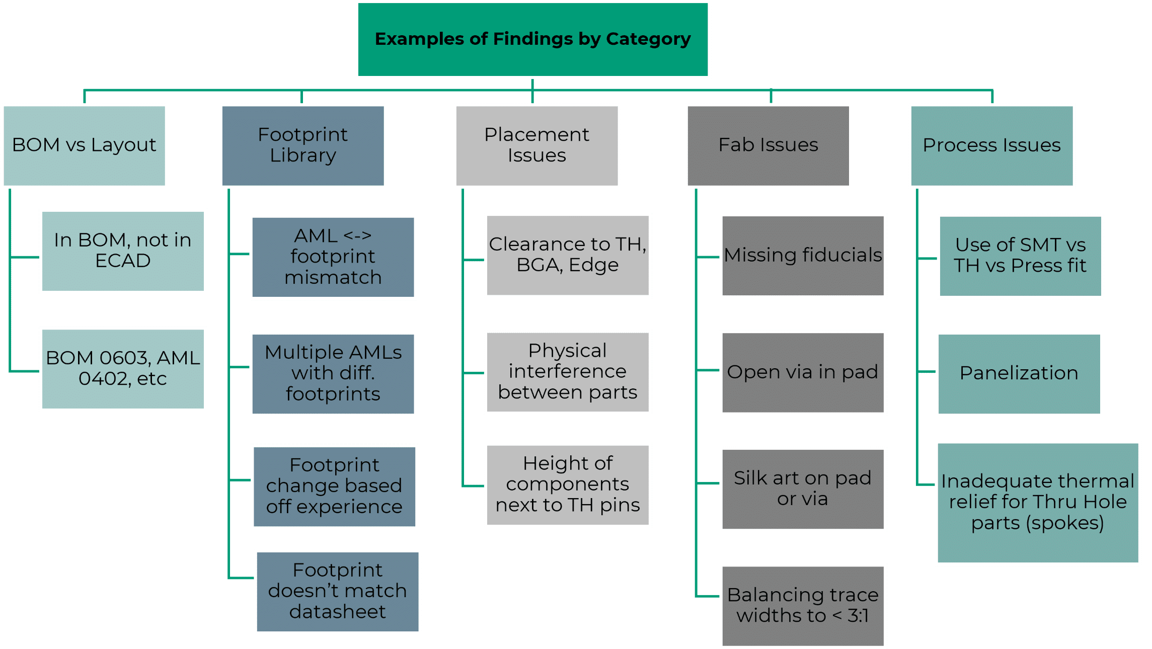
Examples of Feedback by Category
Here are common categories where DFM catches issues before they become build problems:
BOM vs Layout
- Items in BOM but missing in ECAD
- Package mismatches (e.g., 0603 vs 0402)
Footprint Library
- AML ↔ footprint mismatches
- Multiple AMLs with different footprints
- Footprint changes based on experience
- Footprint doesn’t match datasheet
Placement Issues
- Clearance to TH pins, BGA, edges
- Physical interference between components
- Improper height clearances
Fabrication Issues
- Missing fiducials
- Open via‑in‑pad
- Silk art on pads or vias
- Unbalanced trace widths (< 3:1)
Process Issues
- SMT vs. TH vs. press-fit considerations
- Poor panelization strategies
- Inadequate thermal relief for TH parts
What Happens When Issues Are Not Fixed? (Real Examples)
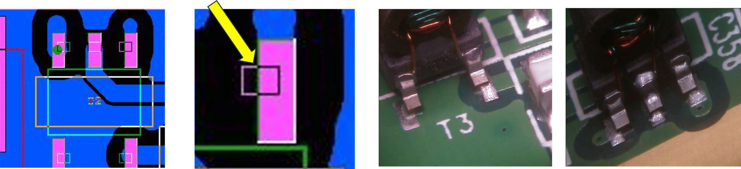
EXAMPLE 1: Insufficient Solder + Poor Alignment
Issue: Component appears to have insufficient solder, and alignment is poor
Findings, Recommendations, and Actions:
- Root cause – bad footprint in CAD
- Customer to fix ECAD library and refresh symbol on the next spin
- Apply correction to all future new boards to prevent repeat issues
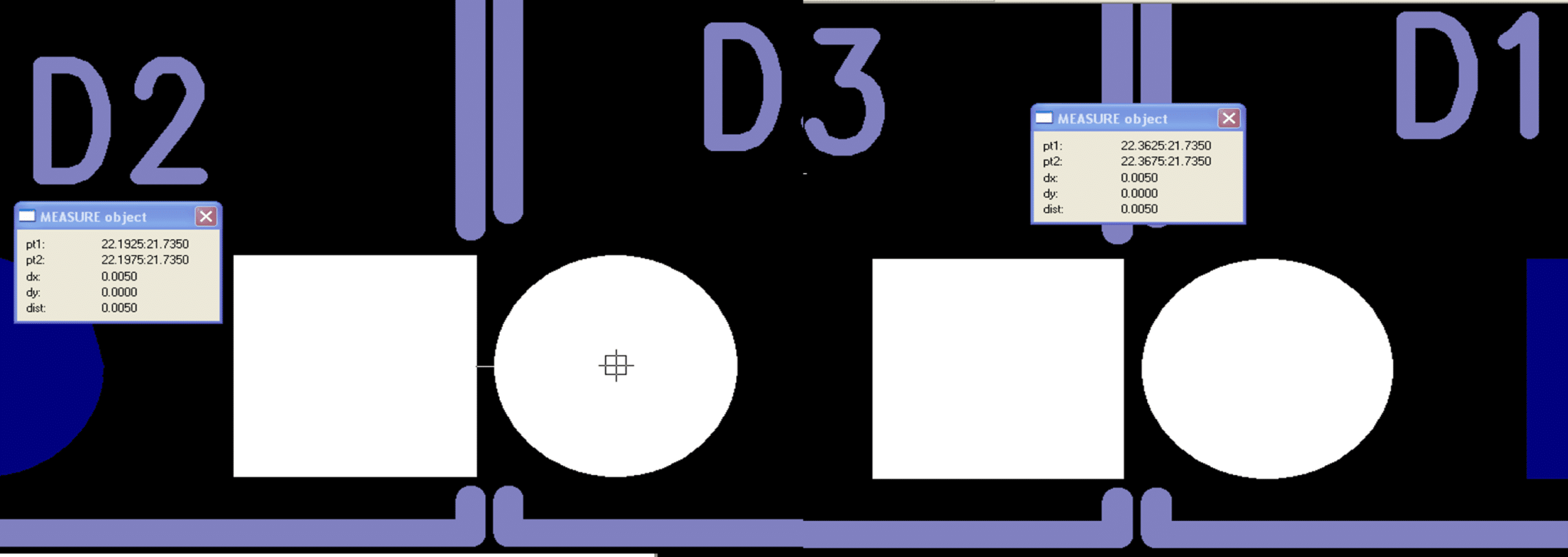
EXAMPLE 2: Solder Bridging Between Adjacent Through-Hole Components
Issue: Solder bridging between two adjacent through-hole components
Findings, Recommendations, and Actions:
- The footprint itself was OK, but the component-to-component spacing was too close
- Move the component on future layouts to increasing spacing
- Customer to add a small keep-out area to the ECAD library to accommodate the solder-wave process and prevent bridging
Quality Data and Analysis: A Passion
We base every recommendation on data, not guesswork.
Depending on site capability and program requirements, analysis may include but not limited to:
- High-level summaries and Pareto charts
- Breakdown by process step
- By job number
- By assembly number
- Trend analysis over time
Quality data drives better decisions, smoother builds, and continuous improvement.

Supporting PPAP & APQP
Successful product realization starts with disciplined planning and controlled execution. In alignment with AS9145 and within site capability and contract scope, we support customer PPAP and APQP activities through structured risk evaluation, including FMEA/PFMEA, collaborative process documentation, control plan development, and expert manufacturability guidance.
These contributions help drive robust qualifications, production readiness, and the process stability required for high-reliability PCBA and Box Build manufacturing.
It Really Makes a Difference!
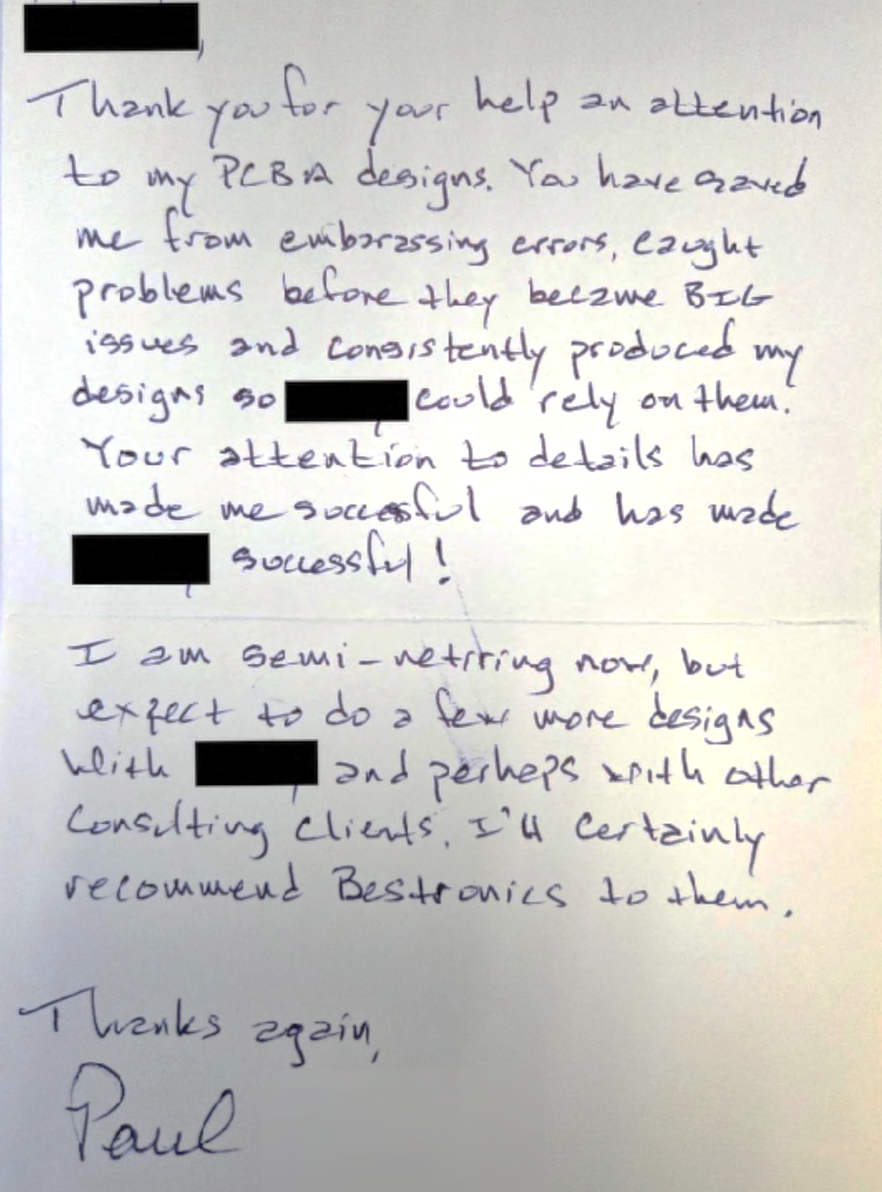
We’ve seen firsthand how DFM involvement transforms outcomes, including an actual letter from a customer engineer thanking the team after DFM-guided changes dramatically improved their yield and reduced rework.
Our teams drive this impact by combining rigorous manufacturability reviews with disciplined production planning and risk management. Through structured DFM engagement, collaborative PPAP and APQP support aligned with AS9145, and proactive risk analysis, including FMEA/PFMEA, we help identify challenges early, strengthen process control, and ensure true production readiness.
Even when design ownership remains with the customer, each site collaborates seamlessly with internal design service locations and trusted external partners to deliver expert insight that improves reliability, manufacturability, quality performance, and launch confidence.
“Bestronics” is now a part of the Emerald Technologies – San Jose Division
Why Are We Passionate About This?
Because saving a small amount of time or money now can cost 10-100x more in the future if DFM is skipped.
A little effort up front prevents:
- Costly re-spins
- Missed schedules
- Manufacturing delays
- Unnecessary scrap and rework
- Field failures
DFM gives you clarity, predictability, and a smoother path to production.
The investment in DFM upfront is always worth it.


